Recent improvements in silicon solar cells promise near-optimal results by cheaper and lighter photovoltaic devices: black silicon front texture, internal light scattering and optimized back reflection.

PhD student Andrea Ingenito has reached 99 percent of the theoretical maximum in light capture in silicon. The Austrian physicist Eli Yablonovitch predicted this limit in 1987, nearly thirty years ago. Until recently, no experiment really came close. But now, Ingenito and colleagues proudly present their black solar cell. Fabricated at Dimes, it’s pushing the theoretical limit.
Ignetio has pulled every trick in the book to maximize light capture in crystalline silicon. His motivation was not (just) an academic contest, the outcome should make photovoltaic cells more efficient and at the same time cheaper to produce.
The challenge that PV manufacturers face is to reduce the amount of material in their products without compromising the efficiency. Yet, the thinner the silicon wafer gets (current industry standard is around 200 micrometer), the less near infrared (800 – 1200 nm wavelength) will be absorbed.
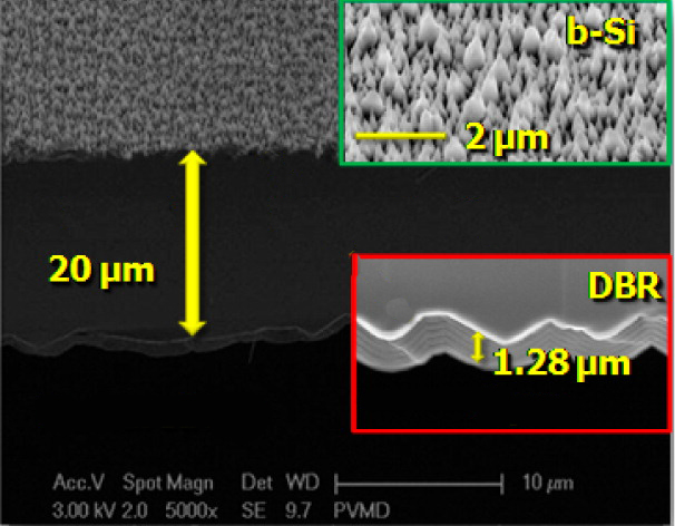
The solution that Ingenito, his colleague Dr. Olinda Isabella and professor Miro Zeman (section photovoltaic materials and devices at the EEMCS faculty) chose was to trap incident light in a 20-micron silicon slice by three measures: a black silicon front, internal dispersion and back reflection.
 Light capture
Light capture
Light capture
Black silicon is a needle-like structure on a silicon surface. It dramatically reduces surface reflection from about 30 percent of a polished wafer to 1 percent. Black silicon – that what it looks like without any reflection – can be made by a standard etching method called reactive-ion etching. The emerging needles measure 1000 nm in height and about 200 nm in diameter. In order to be effective, their dimensions should be smaller than the wavelength they’re meant to couple into the silicon.
Once inside the silicon layer photons are bounced around until they are totally absorbed. The researchers achieved this by structuring the backside of the silicon layer with randomly sized pyramids of which the largest measures 20 microns across and has 5 microns height. The net effect of the uneven back structure is that a large part of the photons that pass through the silicon unabsorbed will be reflected back into the bulk.
Usually, the reflection of the (bumpy) back layer is enhanced by the deposition of a thin silver mirror layer. Ingenito has tried another reflection layer made of a dozen of alternating layers of silicon and silicon-nitride, called a Distributed Bragg Reflector. By properly dimensioning the layers Ingenito managed to maximize the amount of near-infrared photons absorbed in the bulk.
Silver coating performed slightly better than the alternating silicon layers, but DBR has the advantage it’s a silicon-only process, which may prove favorable in production.
 All below
All below
All below
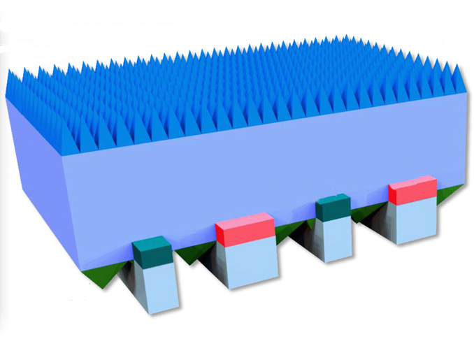
The next step is now to build a photovoltaic device based on this new ultra-thin and totally absorbing material by attaching electrodes to it. The sketch shows that the electrodes are attached under the silicon slice to avoid shadows. Ingenito expects a 30-40 micron black silicon device to feature a light to electron efficiency of about 26 percent. That’s roughly equal to the current record for a wafer twelve times as thick.
Andrea Ingenito, Olindo Isabella and Miro Zeman, Experimental Demonstration of 4n2 Classical Absorption Limit in Nanotextured Ultrathin Solar Cells with Dielectric Omnidirectional Back Reflector, ACS photonics, 13 February 2014
Do you have a question or comment about this article?
delta@tudelft.nl
Comments are closed.